Cleanroom Trends in Semiconductor & Electronics Manufacturing
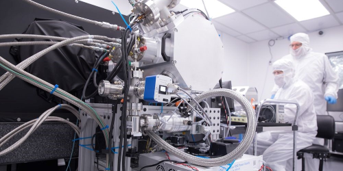
The cleanroom — once a niche concept for pharmaceuticals and biotech — has become the heartbeat of semiconductor and electronics manufacturing. Every wafer etched, every chip assembled, and every sensor packaged happens within environments where even a single dust particle can mean a million-dollar defect.
As India pushes forward with its semiconductor mission, the focus on cleanroom design, performance, and innovation has never been stronger. Globally, the trend is clear: cleanrooms are no longer just controlled spaces — they are becoming smart, energy-efficient, modular, and digitally connected ecosystems.
This article explores key trends shaping cleanroom technology in the semiconductor and electronics sectors, with insights relevant for new fabs, PCB assembly units, display panel manufacturers, and EV battery lines.
The Push for Ultra-Clean Environments (ISO 1–5)
Semiconductor fabrication demands some of the cleanest environments ever engineered. While most electronics manufacturing operates comfortably within ISO Class 6–8, advanced chip manufacturing now requires ISO 1–3, where particle counts are virtually zero.
- ISO 1 Cleanrooms allow less than 10 particles (≥0.1 µm) per cubic meter of air — cleaner than surgical theaters by orders of magnitude.
- Achieving this requires laminar airflow benches, 100% HEPA/ULPA filtration, and multi-zone air handling with pressure cascades as fine as ±2 Pascal.
This push is driven by the miniaturization of chip geometries — today’s 3nm and sub-3nm processes cannot tolerate even molecular contamination. As India’s upcoming fabs under the India Semiconductor Mission (ISM) gear up, the focus on achieving ultra-clean standards is paramount.
Modular & Scalable Cleanroom Construction
Traditional stick-built cleanrooms are being replaced by modular, prefabricated systems.
These offer:
- Faster deployment (up to 40% quicker setup)
- Scalable upgrades as technology nodes advance
- Ease of relocation or expansion
Leading Indian EPC firms now integrate pre-engineered wall panels, ceiling grids, fan filter units (FFUs), and cleanroom coving systems that comply with ISO 14644 while being adaptable to rapid design changes.
A major trend is the hybrid cleanroom model — combining modular construction for critical areas with conventional HVAC zones for support spaces. This approach optimizes both cost and performance — essential for electronics contract manufacturers operating in tight margins.
Energy Efficiency and Sustainable Cleanroom Operations
Cleanrooms are energy-intensive, consuming 30–50 times more power per square meter than standard offices. Semiconductor fabs, in particular, have massive HVAC demands — with 50–70% of total energy dedicated to air filtration and temperature/humidity control.
The global trend — and a growing mandate in India — is green cleanroom design, focusing on:
- Variable Air Volume (VAV) systems to adjust airflow based on load
- Energy recovery wheels in HVAC systems
- Demand-based fan control using particle sensors
- HEPA filter optimization to balance air cleanliness with energy cost
Some next-gen fabs use AI-controlled Building Management Systems (BMS) that automatically adjust temperature, pressure, and filtration levels to minimize power draw while maintaining class integrity.
These energy-efficient designs not only cut costs but also align with India’s Net Zero and ESG goals, which are now influencing site selection and funding eligibility for electronics projects.
Integration of Smart Monitoring and IoT Systems
Modern semiconductor cleanrooms are becoming digitally intelligent.
Sensors, IoT platforms, and cloud-based dashboards continuously track:
- Airborne particle counts
- Temperature and relative humidity
- Differential pressure between zones
- Equipment vibration, static charge, and VOC levels
Deviations trigger real-time alerts and predictive maintenance workflows, reducing downtime and contamination risk.
Data integration with MES (Manufacturing Execution Systems) helps correlate environmental fluctuations with process deviations — a powerful tool for yield optimization.
In India, cleanroom operators in Bengaluru and Noida are already adopting IoT-based cleanroom monitoring suites that use edge computing and AI to ensure regulatory compliance without manual intervention.
Contamination Control Beyond Particulates
In semiconductor and advanced electronics, airborne molecular contamination (AMC) is now as critical as particulate control.
AMC includes vapors, outgassing from materials, acids, bases, and condensable organics that can damage photolithography masks or corrode microcircuits.
Emerging best practices include:
- AMC filtration using activated carbon and potassium permanganate scrubbers
- Low outgassing construction materials (avoiding PVC and silicone-based sealants)
- Dry room conditions (<1% RH) in EV battery and display panel production
The rise of dry cleanrooms for lithium battery manufacturing has brought new challenges — maintaining cleanliness while controlling dew point (< -40°C). These environments demand specialized dehumidification and particle management systems.
Automation and Robotics Inside Cleanrooms
Manual handling is the biggest source of contamination.
That’s why semiconductor cleanrooms are embracing robotics, AGVs (Automated Guided Vehicles), and cobots for wafer transport, packaging, and inspection.
Trends include:
- AMHS (Automated Material Handling Systems) using ceiling or floor-based tracks
- Cleanroom-compatible robots with low particle emission lubricants
- Optical and laser-guided movement systems
In India, upcoming display and PCB assembly units are starting to invest in semi-automated transfer systems, reducing the need for operator entry into critical zones — which directly improves yield and cleanroom longevity.
Localized Clean Zones and Mini Environments
Instead of maintaining an entire hall at ISO 5, manufacturers are increasingly using localized mini-environments — small, self-contained clean zones around critical process tools.
Advantages include:
- Significant energy savings
- Reduced HVAC dependency
- Greater flexibility in equipment layout
These systems combine FFUs, localized air curtains, and positive pressure booths.
In Indian electronics clusters, such as Sriperumbudur and Greater Noida, mini-environments are emerging as a cost-effective alternative to full-scale cleanroom retrofits for SMEs.
Workforce Training and Digital Simulation
Cleanrooms are only as effective as the people managing them.
Global best practices now emphasize virtual simulation, AR/VR-based training, and competency certification for operators, technicians, and facility engineers.
Indian institutes and cleanroom EPCs have started integrating digital twin technology — allowing engineers to simulate airflow, pressure cascade, and contamination scenarios before commissioning.
This ensures both better design decisions and a trained, compliance-ready workforce, aligning with ISO 14644 and IEST (Institute of Environmental Sciences and Technology) guidelines.
India’s Cleanroom Momentum in Electronics Manufacturing
India’s semiconductor and electronics push — backed by ₹76,000 crore PLI and DLI schemes — is catalyzing demand for world-class cleanroom infrastructure.
Sectors leading this growth include:
- Semiconductors and chip packaging
- Display and sensor manufacturing
- EV battery and energy storage systems
- High-end PCB and optoelectronic assembly
Companies like Tata Electronics, Micron, and Foxconn are setting up advanced facilities that integrate GMP-like cleanroom protocols with digital process control.
Local EPC firms are also maturing — offering turnkey cleanroom solutions, integrating HVAC, utilities, process piping, and monitoring systems under one roof.
The Road Ahead
The future of cleanrooms in semiconductor and electronics manufacturing is smarter, greener, and more modular.
We are moving toward:
- AI-driven environmental control
- Carbon-neutral cleanroom designs
- Adaptive filtration systems
- Global harmonization of ISO and local Indian standards
India stands at the cusp of a cleanroom revolution — where the lessons from pharma and biotech sectors merge with the precision demands of nanotechnology and electronics.
As indigenous manufacturing scales up, so will the depth of expertise in contamination control, HVAC design, and digital validation — transforming cleanrooms from compliance assets into strategic enablers of innovation.
Conclusion
Cleanrooms are no longer just sterile boxes — they are intelligent environments engineered for perfection.
In the semiconductor and electronics world, they determine not only product quality but also yield, cost, and competitiveness.
As the global industry converges on India, mastering cleanroom design, validation, and operation will be the key differentiator between manufacturing capacity and manufacturing excellence.